 | |||
|

| Home > Astronomy > Detectors > Site2 |
SITe2 Parameters with UltraDAS
This camera
has been dismantled and therefore no longer exists
Device Identification
|
| Chip name | SITe2 |
| Year of manufacture | 1995 |
| Serial number | 4321ADR01-01 |
| First light on La Palma | December 1997 |
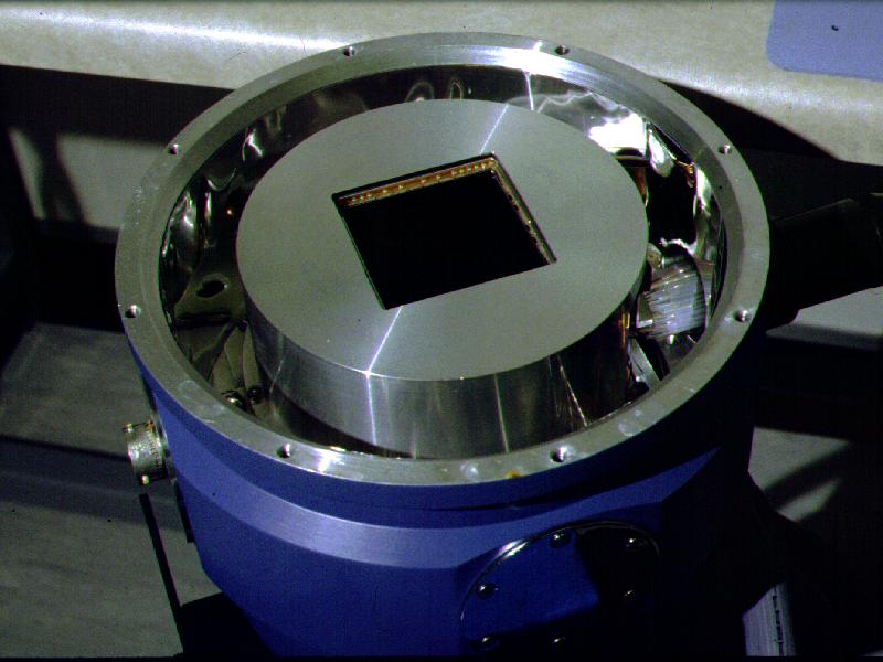
| Description | Photo of Site chip in cryostat. Converted to run with UltraDAS December 2001 |
Operational Characteristics
|
|
|
|
|
|
|
|
|
|
|
|
|
|
|
|
|
|
||
|
|
|
|
|
|
|
|
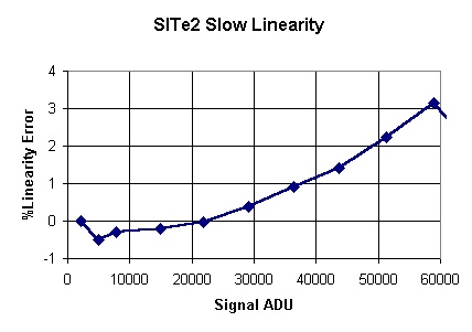
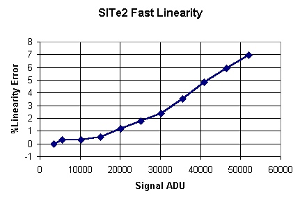
Linearity measurement Courtesy Richard Hijmering using this method
NB For applications requiring good linearity (+/-1%) we recommed that maximum exposure level should be 37000 ADU in slow and 20000 ADU in fast.
Binning in FAST there is no increase in noise up to 4 x 4 binning, in SLOW noise goes up to 7e when 4 x 4 binning is used
NB With the old Dutch controllers the selected readout speed always changed to 'turbo' when binning. This does not happen with the new SDSU controllers, the selected readout speed is not changed. However, the time taken to readout will of course be reduced when binning, as one would expect.
Windowing is available but the first ten columns of the window are noisy.
Example readout times : [1000:1050,1:50]
8 seconds
[1000:1050,1000:1050] 13 seconds
[1000:1050,2000:2050] 18 seconds
| Vertical CTE | 09999993 |
| Horizontal CTE | 0.999999 |
Physical Characteristics
| Pixel Scale (JKT A&G) | 0.33 arc/pixel |
| Field of view (JKT A&G) | 10 x 10 arcmin (unvignetted); 11 x 11 arcmin (vignetted,70% light loss) |
| X Pixel size | 24 microns |
| Y Pixel size | 24 microns |
| X size in pixels of digitised area | 2088 |
| Y size in pixels of digitised area | 2120 |
| X size of useful imaging area | 2048 |
| Y size of useful imaging area | 2048 |
| X start of useful imaging area | 23 |
| Ystart of useful imaging area | 1 |
| LN2 capacity of cryostat | 2.5 litres |
| Cryostat window thickness | 4 mm |
| Distance from window to CCD | 10.3 mm |
| Cryostat window size | 61mm diameter |
Operational Parameters
| Flooding type | none |
| Operating temperature | 168K |
| Preferred amplifier | A, (B is possible backup but noisy >20e) |
| Anti-blooming available | no |
Measured Characteristics
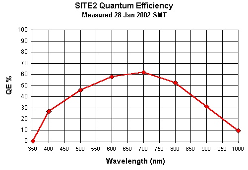
Quantum Efficiency
| Dark current | 1 e/hour |
| Full well bloom limit | 130000 e |
| Chip flatness | 230 micron convex bow |
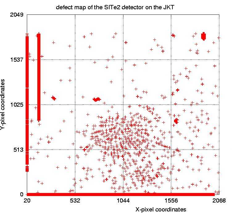
| Cosmetics
|
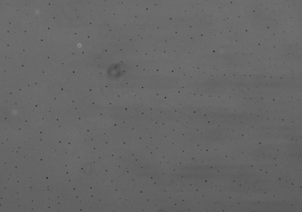
Two blocked column clusters close to edges of chip.
There are several hundred dark spots that cover a large part of the chip, they do however flatfield out please see the defect map Courtesy of Richard Hijmering. |
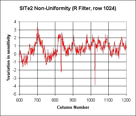
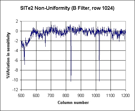
| Non-uniformity | Horizontal cuts across the chip in red and blue. Courtesy Hijmering |
| Top | Back |
|
