 | |||
|

| Home > Astronomy > Detectors > SITe2 |
|
Warning : these figures refer
to SITe2 when it was used with a Dutch controller and
are for reference only.
SITe2 Parameters
Device Identification
|
| Chip name | SITe2 |
| Year of manufacture | 1995 |
| Serial number | 4321ADR01-01 |
| First light on La Palma | December 1997 |
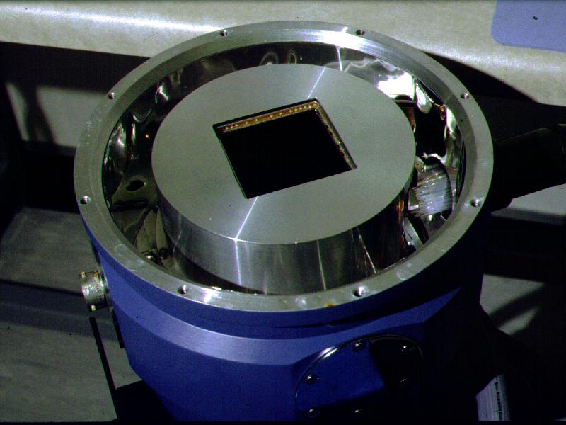
| Description | Photo of Site chip in cryostat |
Operational Characteristics
|
|
|
|
|
|
|
|
| Standard |
|
|
|
|
|
|
| Quick |
|
|
|
|
|
|
| Turbo |
|
|
|
|
|
|
| 2x2 Binned |
|
|
|
|
|
|
| Vertical CTE | 0.9999993 |
| Horizontal CTE | 0.999999 |
Physical Characteristics
| Pixel Scale (JKT A&G) | 0.33 arc/pixel |
| Field of view (JKT A&G) | 10 x 10 arcmin (unvignetted); 11 x 11 arcmin (vignetted,70% light loss) |
| X Pixel size | 24 microns |
| Y Pixel size | 24 microns |
| X size in pixels of digitised area | 2148 |
| Y size in pixels of digitised area | 2148 |
| X size of useful imaging area | 2048 |
| Y size of useful imaging area | 2048 |
| X start of useful imaging area | 20 |
| Ystart of useful imaging area | 1 |
| LN2 capacity of cryostat | 2.5 litres |
| Cryostat window thickness | 4 mm |
| Distance from window to CCD | 10.3 mm |
| Cryostat window size | 80mm diameter |
Operational Parameters
| Flooding type | none |
| Operating temperature | 156K |
| Preferred amplifier | A, (B is possible backup but noisy >20e) |
| Network name | CCD4 |
| Anti-blooming available | no |
Measured Characteristics
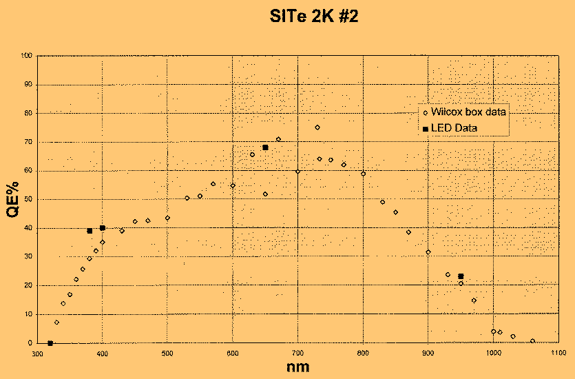
Quantum Efficiency
| Dark current | 1 e/hour |
| Full well bloom limit | 130000 e |
| Chip flatness | 230 micron convex bow |
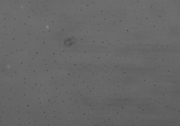
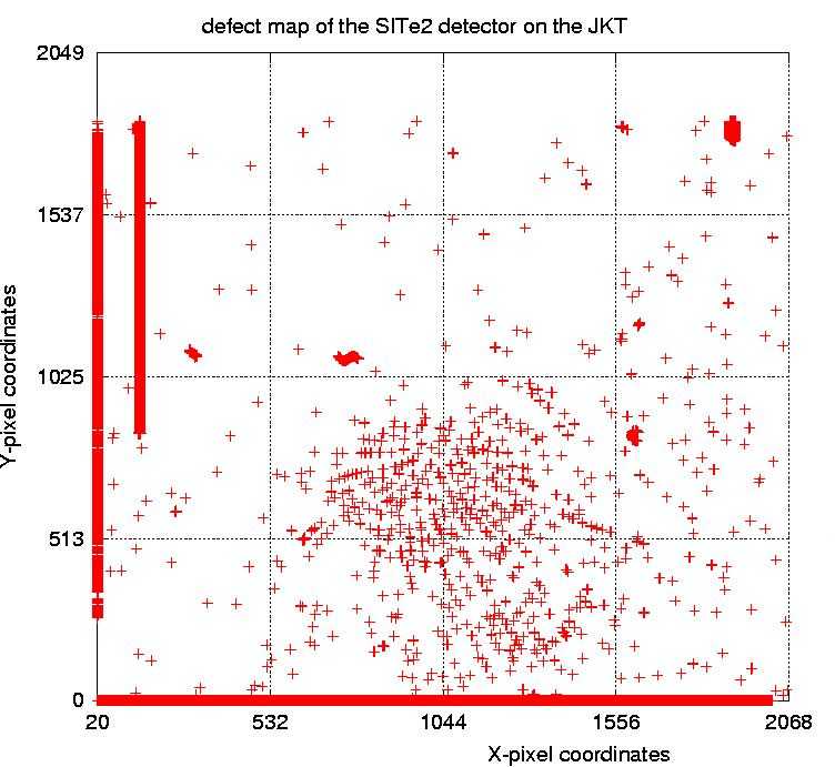
| Cosmetics | Two blocked column clusters close to edges of chip
There are several hundred dark spots that cover a large part of the chip, they do however flatfield out please see the defect map Courtesy of Richard Hijmering. |
| Top | Back |
|
