 | |||
|

| Home > Astronomy > Detectors > FOS1 |
FOS1 Parameters
Device Identification
|
|
|
|
|
|
|
|
|
|
|
|
|
|
|
|
|
|
|
|
|
|
|
|
Vertical CTE 0.999994
Horizontal CTE 0.999996
Physical Characteristics
Pixel Scale ? arcsecs/pixel
X Pixel size 15 microns
Y Pixel size 15 microns
X size in pixels of digitised area 528
Y size in pixels of digitised area 1124
X size of useful imaging area 512
Y size of useful imaging area 1024
X start of useful imaging area 1
Ystart of useful imaging area 1
LN2 capacity of cryostat
2.5 litres
Operational Parameters
Flooding type
Passivated Platinum Process - The high QE of this device in the blue is due to the passivated platinum surface treatment of the CCD. This treatment is particularly prone to surface contamination of the chip such as will occur if the LN2 supply runs out with the chip still cold. If the camera is to be warmed up it is essential therefore that the CCD temperature servo be set to an elevated temperature prior to LN2 exhaustion. If the surface does become contaminated, it will show itself as a loss of blue sensitivity and a very mottled flat field response. The activity of the Platinum treatment can be restored by the following steps :
1) Warm up the camera.
2) Pump for one hour.
3) Backfill the camera through the vacuum pump. This will bathe the chip in dry air since the pump should contain a moisture trap.
4) Leave for one hour, then re-pump for at least a further hour.
5) Refill with LN2 immediately after disconnecting the vacuum pump.
Controller Hardware Modifications CDS Card gain reduced, R5 changed to 6K7
Operating temperature 173K
Preferred amplifier B giving 8.6e noise.( A is the backup giving 8.9 e noise,, C & D are unusable )
Network name CCD1
Anti blooming available no
Measured Characteristics
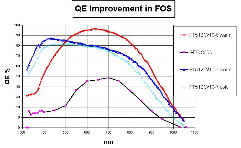
Quantum Efficiency - Sky blue line FT512 W10-7
 Dark current 1 electron/pixel/hour @ -107 Degrees C
after 24 hours in the dark and after being switched on for 16 hours.
Dark current 1 electron/pixel/hour @ -107 Degrees C
after 24 hours in the dark and after being switched on for 16 hours.
Point spread function - The CCD suffers from a poor PSF particularly at the blue end of the spectrum. Photoelectrons diffuse sideways a considerable distance resulting in effective pixel sizes similar to the old GEC chip used in FOS. The FWHM is approximately 1.8 pixels @ 820nm, 2.5 pixels @ 440nm.
Full well bloom limit 50000 e
Chip flatness Approximately +/- 1 micron
Cosmetics - No bad columns, very clean. Thinning defect rounds off the image area near amplifier D, not a serious problem. Some vertical streaks visible in flats near amplifier A. Slight rise in bias in first few columns.
Cosmic Rays 600 events per hour
| Top | Back |
|