3.2. Pixel Response Non-Uniformity.
5. Charge Transfer Efficiency.
Appendices
The camera contains a single EEV-42-80 thinned and AR coated. 13.5mm pixels. 2148 x 4128 pixels total including 50 x-underscan and 50 x-overscan. The active area of the device measures 55.8 x 55.3mm.
CCD Device number : 7061-8-3
Grade 2 device with nine dark columns arranged in three clusters and
no bright columns.
Bright defects :179 total, 48 in central zone. No measurable dark current
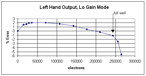
at 120C. Full well 240,000 electrons.
The device was tested using the same operating waveforms as for EEV
#12, the bias voltages however were slightly different.
All test data was recorded at -120C.
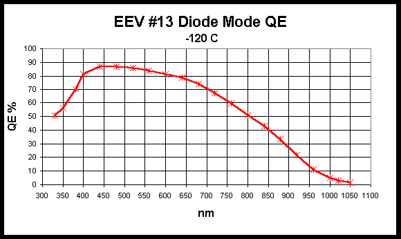
This was measured using a new DC technique and a monochromator to give greater spectral resolution.
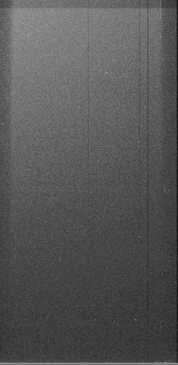
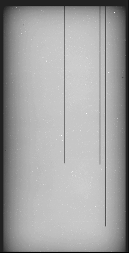
3.1. Image Defects.
The following dark frame is a stack of five 900s dark frames that are
combined to reject cosmic rays. The flat field shows the clustering of
the nine dark columns.
 Dark
Frame Dark
Frame |
 Flat
Field Flat
Field |
Both Images taken with right hand amplifier
|
|
|
|
|
|
|
|
Cosmic ray count is 2000 events per hour.
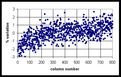
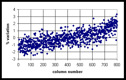
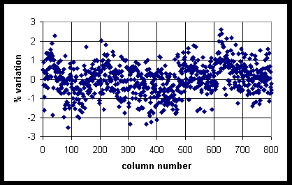
3.2. Pixel Response Non-Uniformity.
This was measured using deeply exposed flat-fields and taking a cut across each image. There was some uneveness in the illumination but the pixel to pixel sensitivity variations are clearly visible. The cross-hatch pattern in the blue flat-field was much less pronounced than with previous 42-80 CCDs. If the chip was illuminated at 950nm with a collimated source, fringes with an amplitude of 14 % were also visible. This fringing does not show in the flat field exposures because the illumination was non-collimated.
 950nm
950nm
 565nm
565nm
 390nm
390nm
The readout noise was characterised for both outputs in both hi-gain and lo-gain mode. These modes were selected by switching the voltage on OG2 so as to vary the output node capacitance.
The output sensitivities of the CCDs are shown below in mV/electron.
|
|
|
|
|
|
|
|
|
|
|
|
The RMS noise is tabulated below for a variety of CDS integration times. In all cases the CDS RC constant was 4.3ms.
|
|
|
|
|
|
|
|
|
|
|
|
|
|
|
|
|
|
|
|
|
|
|
||
|
|
|
Noise and gain are critically dependent on the operational voltages. In particular the output FET drain and image area clock- low should be set to within 100mV of the voltages recommended in Appendix A.
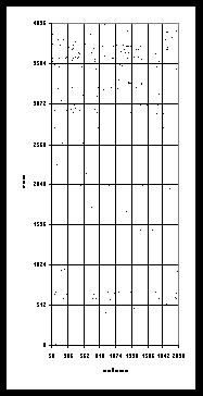
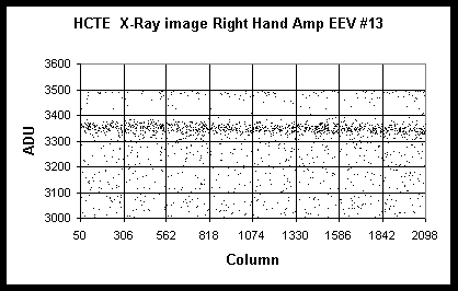
Measured using extended pixel edge response with an exposure of approximately
10,000 electrons. X-ray images were also taken using both outputs when
measuring the gain and noise. The X-ray plots derived from these images
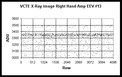
showed very good low level CTE also, although this was not quantified.
| VCTE | HCTE | |
| Left Output | 0.999994 | 0.9999974 |
The Fe55 x-ray plots from the left hand amplifier of each chip are
shown below.
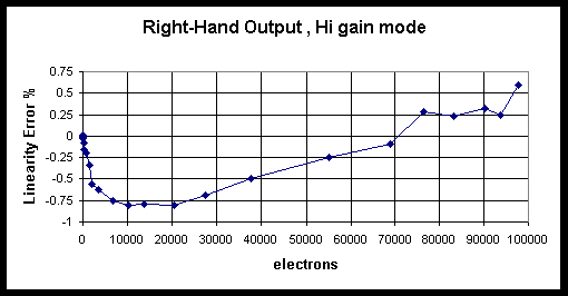
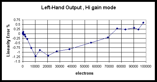
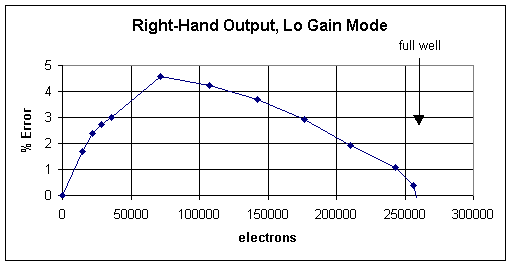
Full well was measured in Lo-gain mode using a pulsed LED source. The point at which the signal became non-linear was coincident with the onset of vertical blooming in the image. The non-linearity associated with the onset of full well had a very 'soft' edge in comparison with other chips. Linearity was excellent from both outputs.
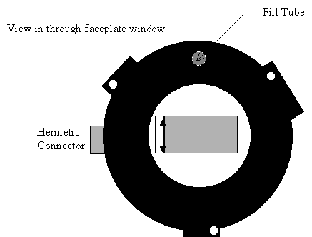
The Camera used a 2.5 l Oxford Instruments blue cryostat. The LN2 hold time when servoing at -1200C with the cryostat vertical , was19.5 hours. The heater servo power required to maintain this temperature was 600mW.
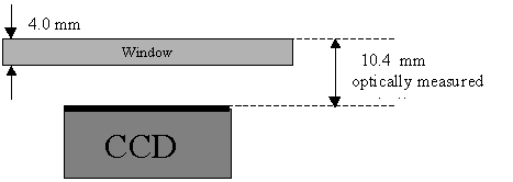
The cryostat window had a thickness of 4mm. The distance from the front face of the window to the surface of the CCD was measured using a travelling microscope.
Appendix A. Operating Voltages
The operating voltages were measured at the pre-amp using a DVM, they are those recomended by EEV .
Image Area clocks :
Lo -15.4V
Hi -3.4V
Serial Register clocks:
Lo - 14 V
Hi - 4.4V
Substrate: -6.4V
OG2 Lo-gain +3V
OG2 Hi-gain -11.4V
OG1 -12.4V
RD +2.6V
OD 13.6V
RPhi :
Lo -12.5V
Hi -3.4V
Dump Drain +7V
The output FET Drain current was set to 2mA.
|
|
|||
|
|
|
||
|
|
|
||
|
|
|
||
|
|
|
||
|
|
|
||
|
|
|
||
|
|
|
||
|
|
|
||
|
|
|
||
|
|
|
||
|
|
|
||
|
|
|
||
|
|
|
||
|
|
|
||
|
|
|
||
|
|
|
||
|
|
|
||
|
|
|
||
|
|
|
||
|
|
|
||
|
|
|
||
|
|
|
||
|
|
|||
|
|
|
||
|
|
|
||
|
|
|
||
|
|
|
||
|
|
|
||
|
|
|
||
|
|
|
||
|
|
|
||
|
|
|
||
|
|
|
||
|
|
|
||
|
|
|
||
|
|
|
||
|
|
|
||
|
|
|
||
|
|
|
||
B Heater -
C LED +
D LED -
E Temp Sense ground
F Temp sense
G Temp sense ref.
H Temp sense +10V