ICD 1.0 version for NAOMI WFS Camera
Part three- Pre-amp circuit, Cabling and Grounding
Xiaofeng Gao
17 January, 2000
Contents list
1.Pre-amp circuit inside the CCD header
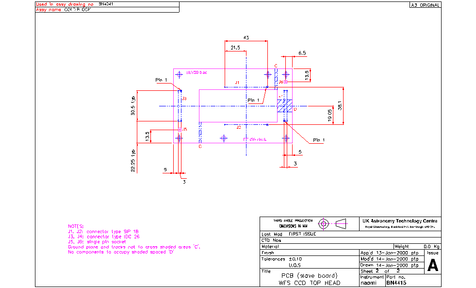
*2. Pre-amp circuit PCB layout
*3. Ground arrangement for the controller
*4. Cabling for video bias and clock from SDSU controller to the CCD header
*5. The new set and old set video cables connection inside SDSU controller
*6. Appendix
*1.Pre-amp circuit inside the CCD header
Four channel single input and differential output pre_amp circuit has been built for NAOMI CCD header. There is also a receiver board built for SDSU controller to enable it to convert the differential signal into single-ended signal. At present system, the pre-amp circuit and the receiver circuit are not used, there are straight line sold on board to pass the circuit.
(U:\sw4\atc_naomi\naomi-0.1\docs\camera\naomi_ICD_parthree.doc ). See enclosed diagram for details (naomipre.prj -Protel file)
there are different layout for master and slave CCD respectively.
(U:\sw4\atc_naomi\naomi-0.1\docs\camera\naomi_ICD_parthree.doc).
See enclosed diagram for details. (bdlayout.vsd-visio file, J1525ch3.pdf-acrobat file)
3. Ground arrangement for the controller
(U:\sw4\atc_naomi\naomi-0.1\docs\camera\naomi_ICD_parthree.doc). See enclosed diagram for details. (naomicable.xls- Excel file)
4. Cabling for video bias and clock from SDSU controller to the CCD header
(U:\sw4\atc_naomi\naomi-0.1\docs\camera\naomi_ICD_parthree.doc). See enclosed diagram for details.(naomicable.xls- Excel file)
5. The new set and old set video cables connection inside SDSU controller
1). The board layout inside SDSU controller
2). The SMA connectors on video board The receiver board for old set cable
3). The 4 black coaxial cables connect to:
|
TR |
TL |
BR |
BL |
|
|
New set |
A1 |
A3 |
A5 |
A7 |
|
Old set |
SMC4 |
SMC3 |
SMC2 |
SMC1 |
|
CCD output (pre_amp board output) |
OS4 (outD1) |
OS3 (OutC1) |
OS2(OutB1) |
OS1(OutA1) |
Circuit board and cabling for NAOMI Camera ==controller
1). Pre-amp board : ONE
put R1,R2,R3,R4,R5,R6,R7,R8,R9,R10,R11,R12,R13,R14,R15,R17 (1M)
c1,c2,c3,c4,c5,c6 (.1uF)
J6,J7,J8,J9,J10,J11,J12,J13 on
sold wire from Pad to Pad( choose as thick as possible)
CA5 to RA6, RA7 to RA2
CB5 to RB6, RB7 to RB2
CC5 to RC6, RC7 to RC2
CD5 to RD6, RD7 to RD2
doc: Bill of Material for M:\ATC\naomi\schemtic\Naomipre.Prj
components for pre-amp board
2). Receiver board : ONE
Put P1 (D50) on, another D9 on see me about that
sold wire from Pad to Pad( choose as thick as possible)
RA1 to TP2
RB1 to TP4
RC1 to TP6
RD1 to TP8
3). Cabling : one set
see naomicable1.xls
Cabling for video and bias
one D50F == AMP26 cable skt (strain relief, RS 450-556, 62GB-585-126S)
one IDC26 skt == AMP26 chassis plug()
four SMA plug == SMB plug (coaxial cable RG174)
200mm
one D25F skt == D9F plus header housing
one D25F skt == the same D9F
Cabling for clock
One D37F == AMP19 chassis skt
One AMP19 cable plug (strain relief )====
AMP19 cable skt (strain relief, RS 450-540, 62GB-585-14-19S)
One AMP19 chassis plug == IDC26 skt