NAOMI WFS CCD - to cool or not to cool.
wht-naomi-86 AOW/WFS/ABG/6.2/7/97/coolccd.doc
Bruce Gentles July 1997
Version 2: Corrected for error in Acquisition photon noise level calc.
The WFS in NAOMI contains a pair of CCD detectors. We have the option to use MPP variants of the CCD and to use a peltier cooler if required. We wish to go for the cheapest option to save money. This report investigates the issues and proposes an approach to adopt.
IMO/non IMO
WE plan to use the EEV CCD39 detector which comes in two variants. The standard CCD can be front or if thinned. back-illuminated We assume the DQE for a thinned sensor.
The chip electrodes can be arranged to have an IMO implant which provides MPP (multi pin per pixel) functionality and has the effect of reducing the dark current by a factor of 100. The terms IMO and MPP are interchangeable.
Making an IMO variant chip is more expensive that the standard chip as a special wafer run has to be done. The IMO variant does not work for the CCD42 which occupies the bulk of this wafer, thus the yield is very low. discussions with EEV indicate that there is ony one spare IMO CCD39 detector in the pipeline which may be needed for the existing Gemini order.
Non IMO/MPP chips are standard parts and are available now.
Information from EEV and DAO on the operation of the IMO variant has revealed that there is a mask problem with the central 2 rows on the CCD, which causes the boundary between these two rows to be ill-defined and the charge divided arbitrarily. The pixel boundary here is also the quadrant boundary and is in the direct centre of the CCD. This means that the centre 2 rows of the CCD do not image properly.
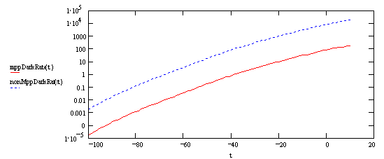
Figure 1 Dark current bulk rates
Cooling
We have the option to cool the chip to reduce dark current. The bulk dark current is a constant rate which is a function of log(t) and the shot noise on the bulk dark current is what affects acquisition as a noise source. The IMO variant reduces this rate by 100 and peltier cooling also reduces the dark current rate.
The dark current limits us in two ways. The bulk dark current uses up valuable pixel full well capacity, and the shot noise adds to the system noise. A practical limit of 2.5 seconds is used to keep the dark signal to below 30,000 ADU for the uncooled non MPP case. All other combinations of MPP and cooling can be integrated for at least 10 seconds without saturation.
CCD package
The chip for the Gemini PWFS has an integral TE cooler in the package. The CCD is in a vacuum to reduce heat loss. To date there have been problems in providing the Vacuum seal for a lifetime of 5 years to meet the Gemini spec.
CCD’s used at ING in the past for Autoguiders have been filled with inert gas , rather than evacuated, and this is all that is considered necessary for our purposes. This should avoid the fabrication problems with the Gemini specification devices. The resulting package will not be as thremally efficient but a slight loss here is not expected to comprimise the acquisition criterion given.
Modelling stellar sources and noise sources.
A MathCad model of the acquisition and AO configurations of the system has been created to estimate the signal and noise levels for different magnitudes of guide star. The model includes atmospheric throughout at 60 degrees zenith distance and the current telescope and AO system optical throughputs.
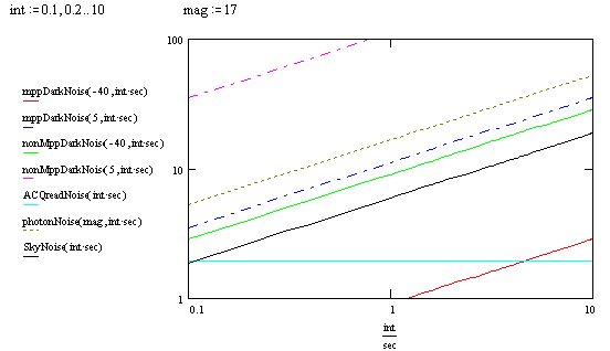 Figure
2 Noise levels
in Acquisition mode
Figure
2 Noise levels
in Acquisition mode
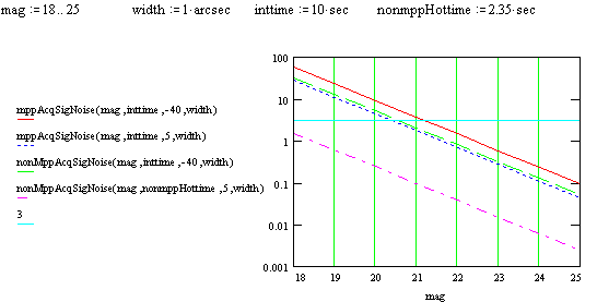
Figure 3 Faint acquisition limits.
Sky background is modelled as a flat source of 20th Mag per square arcsec.
Photon noise is based on a 1 arcsec wide star. There are 0.293 arcsec/pix. Assume that star is flat and 50% of energy is equally distributed over FWHM disk.
Dark current is modelled based on EEV CCD known performance.
Photon noise is modelled as root(signal) and is incorporated via the model used by Nick Dillon for Gemini centroiding analysis.
We have modelled four modes, for MPP and non MPP, and 5 and -40 degrees ccd temperature.
The various noise levels are shown in It can be seen that we are dark current dominated unless we both cool and use the MPP chip.
The photon noise levels are shown for a 17th magnitude star. The equivalent magnitude levels for the dark current noise rates shown are as follows:
|
Mode |
Mv for which |
|
MPP, Cooled to -40 |
23.3 |
|
non MPP, Cooled to -40 |
18.3 |
|
MPP, warm, +5 |
17.8 |
|
non MPP, warm +5 |
12.8 |
The Photon noise in each of the central 4 pixels and the sky noise are similar in level for star of Mv = 19.3
These magnitudes would be the point at which the system would switch from being read-noise/dark current dominated to being photon noise dominated.
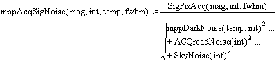
The model incorporates the various sources into a signal to noise metric based on the RMS sum of each of the noise sources. This is simplistic but good enough for these purposes.
The various modes give the following signal to noise curves as a function of source magnitude.
Integration times of 10 and 2.35 seconds are used. Photon noise can be ignored here as we are in the dark and read noise dominates regime.
We can see that the limiting magnitude 3 sigma acquisition is thus approximately Mv = 21.5 for all cases except the non-MPP, uncooled case. This is limited both by the maximum integration time and the large dark current shot noise component.
AO operation
This deals with the case where each subaperture gets 1/54th of the starlight.
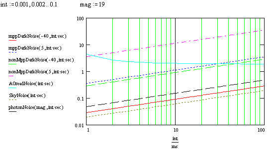
Figure 4 Noise levels in the AO operation mode
I have also developed a related model which deals with the case of operating with an array of subapertures, with 7.35 across the pupil. Here, the signal levels are smaller and the psf is different.
Each subaperture gets 1/54th of the light from the star. I have neglected the partially illuminated ones.
The relative noise levels are shown in
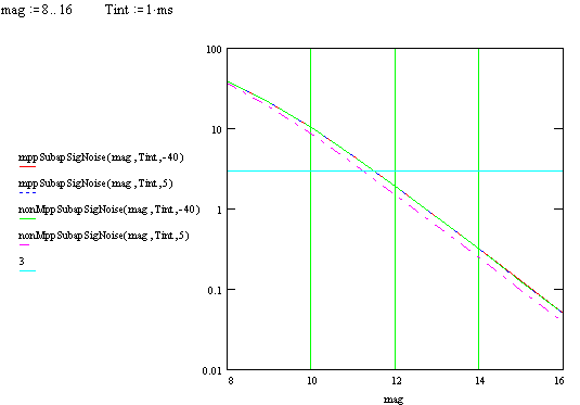
Figure 5 Bright guide star AO limiting magnitude
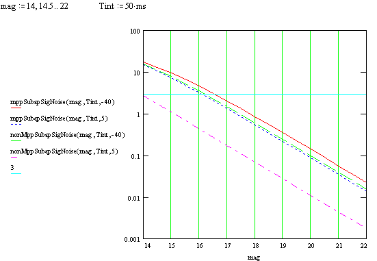
Figure 6 Faint AO limiting magnitude
Discussion
We chose a criterion of having to be able to acquire 19th magnitude science objects. The design aim is to satisfy this with the cheapest solution. This is met by all cases except the uncooled, non MPP CCD.
Also, for AO mode, if we either cool or use MPP then the read noise is dominant over almost all of the operating range of the sensor. These points argue either for cooling or using MPP mode (or both).
The problem with the central rows in MPP mode affects the precise area of the chip which is to be used as the on axis target. This falls in the guard band between the central two rows of subapertures for 4x4 and 6x6 modes. A MPP chip could be used in Shack Hartmann mode. When the WFS is used as a Tip Tilt Sensor or for acquisition, the axis is the target area and is the normal operating area of the CCD. The CCD in MPP mode would thus be useless as a tip tilt sensor unless the MPP problem is fixed. This rules out operation with an MPP device until the mask problem has been corrected.
The difficulties of obtaining any of the current design of MPP devices within our planned project timescale for the WFS mean that we would incur signifnicant technical risk should we choose to use an MPP device for initial operation. If we add to this the technical risks involved in a new mask design on top then it seems unlikely that we would have a fully functional MPP device available for our WFS. It does seem sensible to treat an MPP device as an upgrade to be fitted when available and funds permit. We should certainly consider supporting the correction of the mask defect, funds pernitting as a separate but parallel operation. There may be a solution involving being delivered a non MPP devoce whilst the MPP development work is in progress.
Conclusions
Taking the above factors into consideration, we come to the following conclusions:
1) That we cannot operate with an uncooled, non MPP ccd.
2) That we are unlikely to be able to procure an MPP ccd with correct imaging performance for the initial system.
3) That we should implement a solution with the following characteristics:
· Standard non MPP CCD-39 in Peltier cooler package, inert gas filled.
· Cool the chip to about 45 degrees below ambient.
4) That there are no cost savings to be gained in this area without risking overall system performance or
5) That if funds become available, we should pursue the option of upgrading the device to an MPP variant with the mask defect fixed.
Bruce Gentles 30 June 97.
Models amended 17 July 1997, conclusions unchanged.