
Royal
Observatory, Edinburgh Blackford
Hill Edinburgh,
EH9 3HJ United
Kingdom Telephone: +44
(0)131 668 8100 Facsimile: 668
8264 (Central) 662 1668 (West Wing) 668 1130 (Villas) 662 1654 (Directorate) Email: initial.surname@roe.ac.uk WWW: http://www.roe.ac.uk/
ICD
1.0 version for NAOMI WFS Camera
Part two- VME interface
Xiaofeng
Gao
11
January, 2000
Contents
list
1. Introduction.................................................................................................................................................................. 3
2. References..................................................................................................................................................................... 3
3. The control flowchart.................................................................................................................................................. 3
4. Readout mode [2]......................................................................................................................................................... 4
5. Hardware configuration for synchronized 2-CCD readout................................................................................... 4
6. SDSU VME I/F parallel port and C40 link convert (SDSU-RS422) card interface............................................... 5
7. The data protocol for NAOMI WFS camera............................................................................................................ 6
8. The FSTART and FIFORD waveform....................................................................................................................... 7
9. Error handling............................................................................................................................................................... 8
10. Commands and replies............................................................................................................................................... 9
11. VME I/F board DSP codes for NAOMI WFS camera........................................................................................ 10
12. Modification to SDSU VME I/F board.................................................................................................................. 11
13. CCD readout procedure ( for engineering level).................................................................................................. 13
14. Parameters and memory map for VME I/F board DSP....................................................................................... 14
15. Check for code ID, author and version................................................................................................................. 15
16. Communications between SDSU controller Timing board and VME I/F board.............................................. 15
17. Appendix................................................................................................................................................................... 16
ICD 1.0 version for NAOMI WFS Camera
Part two- VME interface
1. Introduction
This note describes the proposed control flowchart, frame data protocol and commands/replies between host, SDSU VME I/F cards and controller, VME I/F cards and C40 for NAOMI WFS camera. A brief description of communication link between/in SDSU Gen II controller and VME is also included as a background information for understanding the SDSU controller.
2. References
[1] “System description”, SDSU document
[2] “ CCD readout mode”, Derek Ives, UK.ATC
[3] “Timing board”, "VME Interface board", SDSU document Updated MAY,25 1998
[4]“ CCD controller requirements for ground-base optical astronomy” Robert Leach
[5] “ ICD1.6/1.10 Revision Working Document – version 7”, Gemini document
3. The control flowchart
The NAOMI WFS camera system has two CCD headers with two SDSU CCD controllers and two VME I/F cards. They are called master and slave. Each SDSU VME I/F board sits at its own address. The central control system is called Electra ( built in Durham ). The image data is fed from the CCD cameras directly to the ELECTRA system, by-passing the VME bus in the WFS VME control System. The ELECTRA system then performs the image centroiding calculations. Commands are issued from host ( ELECTRA), through Epics/vxWork to call a function from sdsuLib, which communicates with VME I/F board through VMEbus, using a SDSU-defined protocol ( header [source board, destination board , No of words], command and No of arguments if any). The DSP on the VME I/F board checks the in-coming command, it then either goes to a particular subroutine to execute the command, or pass the command to the Timing board (inside controller), which also checks the command and either goes to a particular subroutine to execute the command. When a command is completed, each board (destination board) usually sends a reply back to its source board. The control flowchart is shown in Figure 1.

Figure 1. The control flowchart
4. Readout mode [2]
The different readout modes for Naomi WFS camera are described in more details [2]
5. Hardware
configuration for synchronized 2-CCD
readout
The two controllers in Naomi WFS camera can be operated independently, they then look like just two separate cameras. For synchronized readout, the master and slave controller have to be hardware configured( Figure 2, 3). The “SYNC” signal ( from pin HR/W) by master is hardware decoded to generate an IQRA interrupt to both master and slave ( Figure 2), which will jump to interrupt subroutine once detecting the IQRA. However, the start of synchronized 2-CCD readout is trigged only after a second "SYNC" signal is issued by the master. In order to maximize synchronization for each frame, when the first frame is finished, the slave will wait for a "SYNC" signal issued by the master to start the next frame with the master, and so on.
|
Master Timing board |
||||||||||||||||||||||||

Figure 2 the Master and Slave configuration
 Master: JP16,JP18 and JP21 in
Slave: JP17,JP19
in, R8=50R must be in.
Figure
3 the Master and Slave jump settings
on Timing board
6. SDSU VME I/F parallel
port and C40 link convert (SDSU-RS422) card interface
The image data from CCD controller
will pass SDSU VME I/F card through on board parallel port to C40 array by
SDSU_RS422 interface card. During CCD readout, the DSP on VME I/F board will
generate a “FSTART” signal (pulse) on parallel port as a frame start indication
to SDSU_RS422 interface card in each frame transfer, it will also generate
“RMT_RST” signal on the parallel port, which is then fed back to “FIFORD” as FIFO readout signal to read out
each coming data in FIFO from Timing board.
At the same time, this “RMT_RST” is used as a strobe signal to C40
interface card.
The functional block and
link to SDSU_RS422 card are illustrated
in Figure 4

Figure 4. The function
block and link to SDSU_RS422
The parallel connector on the SDSU VME I/F board is two row 24 IDC type, see below for enclosed photo Figure 5. The pin assignment of the parallel port can be found in SDSU document (vmesch7A.ps)
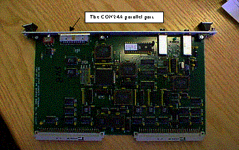
Figure 5. the SDSU VME I/F board
7. The data protocol for
NAOMI WFS camera
Controller to VME I/F board Frame data Format
In response to
readout CCD command, the downlink
(Timing board to VME interface board) is changed from 32-bit to 16-bit format.
The uplink ( VME interface board to Timing board) format remains unchanged
(24bit). The Controller starts to do
CCD readout task. Once the exposure
period has elapsed, 10 of 14-bit header words are transmitted, followed by a
sequence of 16-bit image pixel values. The last 14 bit word in a frame data is
Zero indicating the end of frame. This procedure repeats until an ABORT command
from host is received. The downlink
format is then changed back to 32-bits.
The frame format
is shown in Table 1. It is self-defined
Table 1 Format of Controller Data Frame
|
Word Number |
Name |
Description |
|
0 |
0000 |
|
|
1 |
0000 |
The two zeros are
Frame sync words |
|
2 |
OPMODE |
Repeated here for
sync propose |
|
3 |
OPMODE |
the current
operation mode. DEFINATION [2] |
|
4 |
FRMCH |
Two words for
frame counter, starting from 1, |
|
5 |
FRMCL |
rounded back if
28 bit reached |
|
6 |
EXPSH |
High byte of
the exposure time |
|
7 |
EXPSL |
low byte of the
exposure time |
|
8 |
ROWS |
The number of rows /frame |
|
9 |
COLS |
The number of
columns /frame |
|
1+9 |
PIXEL(1,1) |
First pixel value. |
|
: |
: |
: |
|
N+9 |
PIXEL(4,N) |
Last pixel value. |
|
N+1+9 |
0000 |
End of frame |

N -Number of pixels /frame
VME
I/F board to C40 Frame data Format
In response to
an RDS or RDC command from host, the
VME interface board fiber optic shift register is changed from 32-bit to 16-bit
format. Knowing there is data about to
arrive from FIFO, the DSP on VME I/F board waits, until the beginning of frame
header (0000,0000) is received. It then starts to transmit 7 14- bit header
words to C40, followed by a sequence of 16-bit pixel values. This procedure
repeats until an ABORT command from the host . The fiber optic shift register
then is changed back to 32-bits.
The frame data
format sent to C40 is shown in Table 2.
Table 2 Frame data Format for VME I/F board to C40
|
Word Number |
Name |
Description |
|
0 |
OPMODE |
the current
operation mode. DEFINATION [2] |
|
1 |
FRMCH |
Two words for
frame counter, starting from 1, |
|
2 |
FRMCL |
rounded back if
28 bit reached |
|
3 |
EXPSH |
High byte of
the exposure time |
|
4 |
EXPSL |
low byte of the
exposure time |
|
5 |
ROWS |
The number of rows in frame/frame |
|
6 |
COLS |
The number of
columns in frame./frame |
|
1+6 |
PIXEL(1,1) |
First pixel value. |
|
8 |
: |
: |
|
N+7 |
PIXEL(4,N) |
Last pixel value. |
N -Number of pixels /frame

8. The FSTART and FIFORD
waveform


Timing
|
Timing |
Voltage level on the parallel port CON24 |
||||
|
|
|
D0~D15 ( pin:1-16) |
Voh=2.4v (min) |
Vol=0.4v (max) |
IDT7202 |
|
Tr |
6 ns (min) |
|
Vih=2.0v(min) |
Vil=0.8v (max) |
|
|
Tf |
6 ns (min) |
EF (pin:21) |
Voh=2.4v (min) |
Vol=0.4v (max) |
IDT7202 |
|
Ta |
15 ns
(max) |
FIFORD (pin:19) |
Vih=2.0v(min) |
Vil=0.8v (max) |
CY7C31 |
|
Tdv |
5 ns
(min) |
RMT_RST (pin:17) |
Voh=2.4v (min) |
Vol=0.4v (max) |
DSP |
|
T1 |
Exposure time |
FSTART (pin:18) |
Voh=2.4v (min) |
Vol=0.4v (max) |
DSP |
|
T2 |
21.6 us (min) |
|
|
|
|
|
T3 |
120 ns (min) |
|
|
|
|
|
Tw1 |
40 ns (min) |
|
|
|
|
|
Tw2 |
40 ns (min) |
|
|
|
|
Note: the width of
FSTART and FIFORD, ie, Tw1,Tw2 can be adjusted by user in software.
The measured FSTART
and FIFORD waveform
 Figure 6
The measured FSTART and FIFORD waveform
Figure 6
The measured FSTART and FIFORD waveform
9. Error handling
The error handling in the current system has not yet been fully defined. It is proposed that it will depend on the frame status condition word (FSTAT), which is defined in Table 3
Table 3 Frame Status word bit definition
|
|
Bit |
|
Error |
|
HD_WAIT
|
0 |
Set
if waiting for a frame header, indicates where the DSP is, |
|
|
EOF_ERR |
1 |
Set
if end of frame error |
yes |
|
FBA_VLD
|
2 |
Set
if current frame buffer address is valid |
|
|
LST_FRM |
3 |
Set if last frame or time out |
|
|
ABRT |
4 |
Set
if Abort CMD received during readout |
|
|
TIM_OUT
|
5 |
Set
if time out period 65ms has reached during FIFO readout |
yes |
|
FRDING |
6 |
Set
if frame readout is in process, *this can be changed to anything later |
|
|
FBA_WAT |
7 |
Set
if wait for FBA, only for indication where the DSP is |
|
|
HF_WAT |
8 |
Set
if wait for Half FIFO time out (=FO_TO) |
yes |
The frame status word is only sent back
to Vxwork not to C40
The VME I/F DSP will not take any action apart from reporting during error handling, at any point in reading FIFO, if there is time out, the DSP will jump out, flag Frame status word( FSTAT), send FSTAT back to Vxwork, generate a frame INT, then jump to check CMD routine. The readout process will not stop until it is asked by host to "Abort"
10. Commands and replies
The commands for SDSU VME I/F are listed in BOOT
and APPLICATION tables ( all the command will have a 24 bits header associated
with it, source always is host)
Table 4 SDSU VME BOOT Commands Defined for WFS
|
Command |
Words include
header |
Valid Destination DSPs |
Response |
Description |
|
LDA, Nnnnnn |
3 |
VME | TIMING |
DON |
LoaD Application
program #nnnnnn from EEPROM. |
|
RDM, Maaaaa |
3 |
VME | TIMING |
Dddddd |
ReaD Memory. Read
DSP address maaaaa. Returned data =
dddddd. The most significant nibble
of the address indicates the memory type. m = 1: P memory m = 2: X memory m = 4: Y memory m = 8: EEPROM |
|
WRM, maaaaa,
dddddd |
4 |
VME | TIMING |
DON |
Write Memory. Write dddddd to DSP address maaaaa. The most significant nibble of
the address indicates the memory type. See RDM |
|
TDL, Nnnnnn |
3 |
VME | TIMING |
Nnnnnn |
Test Data Link.
Destination DSP echoes nnnnnn back
to source. |
|
DON |
2 |
VME | TIMING |
DON |
Un-used command |
|
SRA, hiaddr,
loaddr |
4 |
VME |
DON |
Set Reply Address.
Defines the start of a circular buffer in VME memory that receives replies
from the VME interface DSP. |
|
RRS |
2 |
VME |
SYR (fromTiming) |
Remote Reset System.
Reset the Timing and Utility DSPs. |
|
CHK |
2 |
VME |
nnnnnn |
Checksum VME board memory
areas where nnnnnn is calculated value.
|
|
|
|
|
|
|
Notes to Table
1.
“Boot” commands are available on power-up or reset, Checksum will change when new application is
downloaded,
2. all the replies to host are given as they should be. The error replies are given in table 6
3. In NAOMI WFS, we are not using Utility board at all.
Table 5 SDSU VME APPLICATION Commands Defined for WFS
|
Command |
Words Include header |
Valid Destination DSPs |
Response |
Description |
|
ABT |
2 |
VME | TIMING |
DON|DAB (from
VME) |
AborT. Abort the previous RDC/RDS command.
The host should send this command to the VME board only. |
|
RDC |
2 |
VME
| TIMING |
DON (from
VME) |
ReaD CCD.
Put the VEM DSP in readout mode using the current readout sequence and
loaded parameters., wait for frame data from controller, The host should send
this command to the VME board only. |
|
RDS |
2 |
VME
| TIMING |
DON (from
VME) |
Same as RDC but data sent out to C40 through
D24 port |
|
FBA Aaaa,bbbb |
4 |
VME |
NONE |
Aaaa,bbbb=Frame buffer address |
Notes to Table
1. command in an application program which may be either downloaded or loaded from EEPROM using the LDA
2.
all the replies to host are given as they should be.
The error replies are given in table 6
Table 6 SDSU Responses Defined for WFS
|
Response |
Description |
|
DON |
DONe. Command received and processed without
error. |
|
DAB |
Done Abort during readout |
|
SYR |
System Reset. The controller has reset
(power-on reset, reset button, RRS reset, or watchdog timer reset). |
|
|
Error message |
|
ERR |
ERRor. Unrecognized command |
|
POE |
Power On Error. Error occurred while powering
up the analog supplies on the utility board. |
|
AFE |
Address Format Error. A valid P, X, Y or
EEPROM address was not specified. |
|
HDE |
HeaDer Error. The first word in the command
has error |
11. VME I/F
board DSP codes for NAOMI WFS camera
The DSP code
developed for NAOMI WFS camera consists of three parts:
1). Boot code
vmeboot.asm
2). Head code vmehead.asm
3). Application code vmeapl1.asm, vmeapl2.asm and vmeapl3.asm
vmeapl1.asm application 1
is used for reading out data to VxWork , the image can be displayed on SAOtng window and saved into a file.
vmeapl2.asm application 2
is used for reading out data to C40. No data can be seen by VxWork apart from frame state word (SFTAT)
vmeap3.asm application 3
is used for self test for VME I/F board. The simulated image can be displayed on SAOtng window and saved into a file.
Makefile
Three makefiles are available to use: (details seen Appendix)
1). Make -f makenorm.mk è vmebt_norn.s, vme_norm.s
compilers and links vmeboot and applications. Later, *.s files are programmed into an E2prom (28c256) by a normal programmer.
2). Make -f makeevm56k.mk è vme56k.cld
compilers and links vmeboot and applications. Later, *.cld file is programmed into an E2prom (29c256, 27c256) by a motoroal 56k Evaluation Module board
3). Make -f makedownload.mk è vmeapl (1/2/3)_dwld.lod
compilers and links only applications. Later, *.lod files are downloaded directly into the DSP.
The DSP code flowchart is illustrated in Figure 7.
12. Modification to SDSU VME
I/F board
It was discovered during the project that
SDSU VME I/F board did not have a hardware means to detect whether a request of VMEbus interrupt has been granted.
Various tests by a VME bus analyzer have illustrated that there could be a few
microseconds delay for VME CPU board to respond to a VMEbus interrupt. To make the system more reliable, a
modification to SDSU VME I/F board has been made. The wire links added to SDSU VME board are:
Ø
wiring DSP
portB.6 (DSP pin 15) to U33 pin 8
(internal connected to U22 pin5)
Ø
for INT IRQ
monitor
> wiring DSP
portB.8 (DSP pin 7) to parallel port pin 18 for FSYNC
> wiring DSP
portB.10 (DSP pin 4) to U30 pin 9 for
FF
see the following
diagram


Figure 7 the VME I/F DSP code flowchart
13. CCD readout procedure (
for engineering level)
At engineering level, the system setup without C40 is shown in Figure 8

Figure 8 the system setup without C40
Starting a CCD readout task involves three scripts at low level (VxWork):
1). Task
includes to startup Vxwork or Epics,then, startup sdsulib tasks, download DSP codes into VME I/F and Timing boards
2). Initial
setup parameters for VME I/F ,Timing DSP code and memory buffer in VME,
3). Read
start the CCD readout.
An example of CCD readout is of something like:
From a Xterm window,
type telnet naomi (could be another name),
type <startup.
Then type <startCCDReadout (see detail in Appendix )
There are few useful sdsuLib commands for engineering level ( details see sdsuLib manual ):
1). SdsuFrameShow "cam1" or sdsuCurrentFrameShow "cam1" ( cam1 is the name
for Master/slave )
display the frame status word and header
information, the address where the
frame data is stored
2).sdsuDebug
if sdsuDebug=1, there will be printed message on screen when a frame interrupt occurs, set sdsuDebug=0, will disable the function. It gives visible way to see if the frame readout is happening .
3). SdsuCommand ("cam1",1,"ABT")
this will abort the CCD readout task
4). To read parameter
sdsuMemory (“cam1”,1,”RDM”,”CODE_ID”) or sdsuCommand (“cam1”,2,”RDM”,0x******,0)
(where ****** is the address for P:10***, X: 20****, Y:40****,EEP:80****)
5). to write parameter
sdsuMemory (“cam1”,2,”WRM”,”EXP”) or sdsuCommand (“cont1”,2,”WRM”,0x******,0)
(where ****** is the address for P:10***, X: 20****, Y:40****,EEP:80****)
14. Parameters and memory map for VME I/F board DSP
Table 7 the
effects of different setting in parameters on VME DSP code
|
|
|
Effects |
|
|
DSPOCODE (in Y: memory) |
Bits |
|
|
|
WHICH |
0 |
=0 donot send
RDC to TIMing board, =1 send RDC to
TIMing board, remove 12 garbage from frame data |
|
|
RDHEAD |
1 |
=0 donot check header, =1 check header |
|
|
TWOPMD |
2 |
=0 only one opmode in the header =1 two opmode in header |
|
|
DOPIXC |
3 |
=0 donot calculate PIXELC, use PIXEL_N set in
initial by user =1 calculate PIXELC=rows*cols |
|
|
TIMCK |
4 |
=0 don't do time out for Half fifo full =1 do FO_TO time out check half fifi full |
|
|
GARBAGE |
5 |
=0 no garbage in data from Timing board
code =1 remove NOFGAR garbage from frame data in
Timing board code |
|
|
|
|
|
|
|
CHKPXY (in
X: memory) |
Bits |
|
|
|
CHKP |
0 |
Do checksum for p memory ($0…$chk_sum) |
|
|
CHKX |
1 |
Do checksum for p, X memory ($0…$chk_sum, x) |
|
|
CHKY |
2 |
Do checksum for p,Y memory ($0…$chk_sum, y) |
|
|
|
|
|
|
|
FSTAT_WIDTH |
|
The frame start pulse for C40, unit=0.04us. default=2000 |
|
|
READ_WIDTH |
|
The READ FIFO pulse width for C40, unit=0.04us.
default=5 |
|
Table 7 the Memory map for VME DSP code( all in HEX number)
|
|
56KVME
memory location (
word wide ) |
length(word) |
EPROM
memory Location (byte
wide) |
length |
Difference in Words |
DSP memory Location |
|||
|
progvme.asm |
upwards |
7F00 |
|
|
|
|
|
|
|
|
vmeboot.P |
(BOOT_P) |
2000 |
(BTLH_P) |
0300 |
(EEPO_P) |
C000 |
|
|
P:RST_ISR |
|
vmeboot.X |
(BOOT_X) |
2300 |
(BTLH_X) |
0100 |
(EEPO_X) |
C900 |
0900 |
|
X:XPARAMT |
|
vmeapl1.P |
(APPL1_P) |
2400 |
(APLH1_P) |
0200 |
(EEAP1_P) |
8000 |
|
0000 |
P:APL_ADR |
|
vmeapl1.X |
(APPL1_X) |
2600 |
(APLH1_X) |
0100 |
(EEAP1_X) |
8600 |
0600 |
0200 |
X;USR_CMD |
|
vmeapl1.Y |
(APPL1_Y) |
2700 |
(APLH1_Y) |
0100 |
(EEAP1_Y) |
8900 |
0300 |
0300 |
Y:0000 |
|
vmeapl2.P |
(APPL2_P) |
2800 |
(APLH2_P) |
0200 |
(EEAP2_P) |
8C00 |
0300 |
0400 |
P:APL_ADR |
|
vmeapl2.X |
(APPL2_X) |
2A00 |
(APLH2_X) |
0100 |
(EEAP2_X) |
9200 |
0600 |
0600 |
X;USR_CMD |
|
vmeapl2.Y |
(APPL2_Y) |
2B00 |
(APLH2_Y) |
0100 |
(EEAP2_Y) |
9500 |
0300 |
0700 |
Y:0000 |
|
vmeapl3.P |
(APPL3_P) |
2C00 |
(APLH3_P) |
0200 |
(EEAP3_P) |
9800 |
0300 |
0800 |
P:APL_ADR |
|
vmeapl3.X |
(APPL3_X) |
2E00 |
(APLH3_X) |
0100 |
(EEAP3_X) |
9E00 |
0600 |
0A00 |
X;USR_CMD |
|
vmeapl3.Y |
(APPL3_Y) |
2F00 |
(APLH3_Y) |
0100 |
(EEAP3_Y) |
A100 |
0300 |
0B00 |
Y:0000 |
15. Check for code ID,
author and version
Every VME DSP
code has a version. The CODE_ID and
AUTHOR are only in boot code. Use sdsuMemory (“cam1”,1,”RDM”,”xxx”),
where xxx is the symbol
|
symbol |
Expected
reply |
Version
XX.XX |
board
XX |
Or Application XX |
|
CODE_ID |
"ATC" |
|
|
|
|
AUTHOR |
"GAO" |
|
|
|
|
BT_CODE_VER
|
$010001
|
1.00 |
01
= VME Rev. 7A |
|
|
APL_CODE_VER
|
$010001
|
1.00 |
|
01=
application 1 |
16. Communications between
SDSU controller Timing board and VME I/F board
|
|
||||||||||||

Details for the communication between the VME board and the Timing board
|
clock board SSI
serial 3.1Mbits/s
[4] |


The SDSU system processor block and communication path [3] . The boards in dash line only
for CCD operation reference.
17. Appendix
1). Make files
makeevm56k
#!/bin/csh
clear
echo
" This generates NAOMI VME DSP release version 1.00 boot code plus
applications, "
echo
" programed by
56kVME ==> vme56k.lst,.cld,vme56k.lod "
echo
"PRGAPL BOOT/APL1/APL2/APL3
program onlyboot/application1/2/3 "
echo
"PRG EVM56K program boot CODE for EVM56K vmeboot_56k.lst"
echo
"PRG EVM56K program application CODE for
EVM56K/"
echo
"
vmeapl1_56k.lst
vmeapl2_56k.lst vmeapl3_56k.lst "
echo
" X.Gao
26-11-99 at ATC
"
asm56000 -b -lvme56k.lst -d PRGAPL APL1 -D PRGAPL2 APL2 -D PRGAPL3 APL3 progvme.asm
asm56000 -b -lvmeboot_56k.lst -d PRG EVM56K vmeboot.asm
asm56000 -b -lvmeapl1_56k.lst -d PRG EVM56K -d TEST HEAD -d READ MAUNAL vmeapl1.asm
asm56000 -b -lvmeapl2_56k.lst -d PRG EVM56K -d TEST HEAD -d READ MAUNAL vmeapl2.asm
asm56000 -b -lvmeapl3_56k.lst -d PRG EVM56K -d TEST HEAD -d READ MAUNAL vmeapl3.asm
dsplnk -bvme56k.cld -v progvme.cln vmeboot.cln
vmeapl1.cln vmeapl2.cln vmeapl3.cln
rm
vme56k.lod
cldlod vme56k.cld >vme56k.lod
rm *.cln
makenorm
#!/bin/csh
clear
echo " This generates NAOMI VME DSP release
code version 1.00 boot code plus applications,"
echo " programed by NORM programmer vmebt_norm/vme_norm.lst,.cld,vmebt_norm/vme_norm.lod"
echo " PRGAPL BOOT/APL1/APL2/APL3 program onlyboot/application1/2/3 "
echo " PRG
NORM program boot CODE
for NORMAL EEPROM "
echo " PRG
NORM program application
CODE for NORMAL EEPROM "
echo " X.Gao
26-11-99 at ATC"
echo "
BOOT first ==>
vmebt_norm.s"
asm56000 -b -lvmebt_norm.lst -d PRG NORM vmeboot.asm
dsplnk -bvmebt_norm.cld -v vmeboot.cln
rm
vmebt_norm.lod
cldlod
vmebt_norm.cld >vmebt_norm.lod
srec
-bs vmebt_norm.lod
echo
" Now APPLICATIONS
==> vme_norm.s"
asm56000 -b -lvmeapl1_norm.lst -d PRG NORM -d TEST HEAD -d READ MAUNAL vmeapl1.asm
asm56000 -b -lvmeapl2_norm.lst -d PRG NORM -d TEST HEAD -d READ MAUNAL vmeapl2.asm
asm56000 -b -lvmeapl3_norm.lst -d PRG NORM -d TEST HEAD -d READ MAUNAL vmeapl3.asm
dsplnk -bvme_norm.cld -v vmeboot.cln
vmeapl1.cln vmeapl2.cln vmeapl3.cln
rm
vme_norm.lod
cldlod vme_norm.cld >vme_norm.lod
srec -bs vme_norm.lod
rm *.cln
makedowload
#!/bin/csh
clear
echo " build download version of VME
application3 DSP code for VME board"
echo
"
<<<<< DOWNLOAD VERSION >>>>> "
echo
" vmeapl1_dwld.lod vmeapl2_dwld.lod vmeapl3_dwld.lod"
echo
" X.Gao 26-11-99 at ATC"
#vmeapl1_make
clear
echo NAOMI
VME application1 DSP code for VxWork, host sends RDC to VME
echo " <<<<< DOWNLOAD VERSION
>>>>>
vmeapl1_dwld.lst, vmeapl1_dwld.lod "
echo " X.Gao
26-11-99 at ATC
"
echo off
asm56000 -b -lvmebootdwld.lst -d PRG NORM vmeboot.asm
asm56000 -b -lvmeapl1_dwld.lst -d PRG
DOWNLOAD -d TEST HEAD -d READ MAUNAL
vmeapl1.asm
dsplnk -bvmeapl1_dwld.cld -v
vmeapl1.cln vmeboot.cln
rm
vmeapl1_dwld.lod
cldlod vmeapl1_dwld.cld >vmeapl1_dwld.lod
#vmeapl2_make
clear
echo NAOMI
VME application2 DSP code for C40, host sends RDS to VME
echo
"<<<<< DOWNLOAD VERSION >>>>> vmeapl2_dwld.lst, vmeapl2_dwld.lod"
echo
" X.Gao 26-11-99 at ATC"
echo off
asm56000 -b -lvmebootdwld.lst -d PRG NORM vmeboot.asm
asm56000 -b -lvmeapl2_dwld.lst -d PRG
DOWNLOAD -d TEST HEAD -d READ MAUNAL
vmeapl2.asm
dsplnk -bvmeapl2_dwld.cld -v
vmeapl2.cln vmeboot.cln
rm
vmeapl2_dwld.lod
cldlod vmeapl2_dwld.cld >vmeapl2_dwld.lod
#vmeapl3_make
clear
echo NAOMI
VME application3 DSP code for VME board selftest, host sends RDC to VME
echo
"<<<<< DOWNLOAD VERSION >>>>> vmeapl3_dwld.lst, vmeapl3_dwld.lod"
echo
" X.Gao 26-11-99 at ATC"
echo off
asm56000 -b -lvmebootdwld.lst -d PRG NORM vmeboot.asm
asm56000 -b -lvmeapl3_dwld.lst -d PRG
DOWNLOAD -d TEST HEAD -d READ MAUNAL
vmeapl3.asm
dsplnk -bvmeapl3_dwld.cld -v
vmeapl3.cln vmeboot.cln
rm
vmeapl3_dwld.lod
cldlod vmeapl3_dwld.cld >vmeapl3_dwld.lod
2). StartCCDReadout
# startup task
sdsuCommandStart ("cam1", 0xc0000000, 0)
sdsuMemoryStart ("cam1")
sdsuReadoutStart ("cam1")
sdsuMemory ("cam1", 1, "FDL",
"/sw4/naomi/naomiWfs/dsp_code/xg/finalversion/vmeapl1_dwld.lod")
# initialise
sdsuCommand ("cam1", 2, "PON",
0, 0)
sdsuCommand ("cam1", 2, "SET",
100 , 0, 0)
sdsuMemory ("cam1", 1, "WRM",
"DSPCODE", 46 )
sdsuMemory ("cam1", 1, "WRM",
"PIXEL_N", 7040 )
sdsuMemory ("cam1", 1, "WRM",
"FSTAT_WIDTH", 10)
sdsuMemory ("cam1", 1, "WRM",
"NOFGAR", 8)
sdsuReadoutFrameQ ("cam1", 7040, 5)
sdsuCommand("cam1",2,"SYC",0,0)
# start readout of application 1
sdsuReadoutRDC("cam1", 50)
sdsuCommand("cam1",2,"LDA",1,0)
sdsuCommand("cam1",2,"SYC",0,0)
3). Default jump setting (most see SDSU VME Doc)
board address=0xc0000000 ( A31,A30 out, the rest in)
fiber optic speed =50MHz
address modifier=$
interrupt level=6 (IRQ6 in, IACK0 in, others out)
bus request level =3
Eeprom =29c256( the same setting as 27c256), JP1 (1=2) JP2(1=2)
Watch dog timer = disabled
4). Example of test
login coll
startup another xterm
telnet naomi - can now communicate with VME rack
<startup
to display images
-----------------
startup another xterm
source /net/alba/sw4/naomi/naomilogin
naomiQI
a SAOTNG should become active
to start the VME self test
readout process
----------------------------
naomiCam - cd "/sw4/naomi/naomiWfs/scripts/xg"
naomiCam -<xgVMEC40test
then you will see an image on SAOtng window.
naomiCam -sdsuDebug=1
will display the frame interrupt message, indicating the working
condition
naomiCam -sdsuDebug=0
will stop
naomiCam - sdsuFrameShow "cam1"
Contents of SDSU frame located at
: 0xeb0000
Frame message queue :
0xef3fc8
Frame semaphore ID :
0xef7010
Frame header, located at address
: 0xeb0008
Packet count : 209
Frame start count : 0
VME board count : 0
Timing board count :
0x13b68
Frame status : 0xc0
Operation mode : 0x1
Exposure time :
0xf4240
Number of rows : 78
Number of columns : 86
First 8 pixels, located at address : 0xeb0020
1234 5678 1357 2468 1234 5678 1357 2468
to start the VME/Timing self
test readout process
----------------------------
<xgVME_cam1_dummy ( for
dummy star)
<xgVME_cam1_mode7 ( for simulated data)
to start the VME/Timing readout process
----------------------------
<xgcam1Rd_Vx