NAOMI Electronic systems Overview
11th August 2000
wht-naomi-13
Contents
1. Electronics Rack Page 3
1.1 CCD Controller PSU Page 3
1.2 Peltier PSU Page 4
1.2.1 Interlock circuit Page 4
1.3 Fan tray Page
4
1.4 CCD VME Crate Page 4
1.5 NAOMI VME Crate Page 5
1.5.1 Motor Controllers Page 5
1.5.2 Digital I/O Card Page 6
1.5.3 Waveform Generator card Page 7
1.5.4 Thermocouple Board Page 7
1.6 PSU Module Page 7
1.6.1 Relay Card Page
7
1.6.1.1 DC Motor Page 8
1.6.1.2 Shutter Control Page 8
1.6.2 Vexta Drive card Page 9
1.6.3 Newport Drive Card Page 9
1.7 Berger Lahr motor drive
modules Page 10
1.8 FSM Filter Page
10
1.9 FSM Electronics Page 11
2.0 Calibration unit Page 12
2.1 The Mask stage Page
12
2.2 Beam Splitter Stage Page 12
2.3 Calibration Shutter Page 12
2.4 Tip/Tilt Mirror Page 12
3 Wave Front Sensor Page 13
4. Optical Mechanical
Chassis Page 15
Appendix
I Spares List Page
16
Appendix
II Temporary set up of Rack Page 17
List of
Figures
Figure
1. Electronics Rack Page 3
Figure
2. DC Motor Control Page 8
Figure
3. Shutter Control Page 9
Figure
4. FSM Filter Block Diagram Page 10
Figure
5. WFS Block Diagram Page 13
Figure
6. Switch Logic for WFS Page 15
List of
Tables
Table
1. VME Rack Page
5
Table
2. Motor Axis Page
6
Table
3. Digital Input / Output
Bits Page 6
Table
4. PSU Module Page 7
Table
5. WFS Switches Page 14
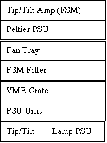
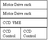
1: Electronics Rack
The electronics rack houses the power supplies and control for the
NAOMI systems. The layout of the rack is illustrated in Fig 1 below and each
section will be described.
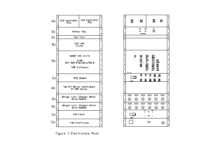
Figure 1 Electronics Rack
1.1: CCD Controller PSU
The CCD Controllers sit on the Optical Bench next to the WFS. The power for the controllers is supplied from two units that sit beside each other on a tray in the electronics rack. The connections from the supplies go directly from each of these units, out the back of the rack and to the associated controller, one for each CCD.
1.2: Peltier PSU : 16-07e4.sch
The Peltier PSU rack provides
power to the peltier devices that are attached to the CCD heads. Cooling flows
round the heads and controllers. To prevent the power being switched on whilst
there is no cooling the power supplies are interlocked with the compressor. A
flow meter is attached in line with the cooling lines and provides a signal
when there is a flow, where the frequency of the signal is proportional to the
flow rate.
The peltier psu rack contains three power supplies, two 12V, one 5v, a solid state relay (SSR), the interlock circuitry and load resistors. When the unit is switched on the 12v supplies, which provide power to the peltiers via the CCD controllers will only be powered up via the SSR if there is coolant flow. The 5v power supply provides the power for the circuitry and the flow meter. The output of the flow meter, which is a square wave, is fed to the interlock circuitry, if the flow is high enough a signal will be sent to the SSR switching on the 12v supplies.
The peltiers require a constant current of about 3A @ 2.5V. This is achieved by regulating the voltage before it goes to the controllers. Due to the high current and the length of cable there is a considerable voltage drop along the lines, this however was not enough to reduce the voltage so resistors were added in the rack adding 1.5W to the line resistance. This then reduces the voltage enough to feed the regulator. The regulator then gives a fixed current of 3A, which is fed into the CCD controllers.
1.2.1: Interlock circuit : 16-07e4.sch
When the coolant flow is high enough to provide sufficient cooling the output from the flow meter is about 60Hz. This is a +/- square wave, which is transferred to a TTL signal (0 to +5v). This is then fed to a frequency to voltage converter, the output of which is compared with a fixed voltage level. The level for the comparitor is set to just below the level given by the F-V converter thus allowing for small fluctuations. When there is sufficient flow and the output of the F-V converter is higher than the reference level the output of the comparitor will be high closing the SSR, which will switch on the 12V power supplies. If the flow drops the comparitor will go low and the supplies will be switched off.
1.3: Fan Tray
The fan tray has six fans to provide cooling for the peltier PSU rack above.
1.4: CCD VME Crate
1.5: NAOMI VME Crate : 00-07e8.dwg
The NAOMI VME crate consists the following cards;
|
CARD |
NAME |
DESCRIPTION |
|
MVME 167 |
Processor Card |
|
|
MVME 712 |
Translation board |
|
|
VME 8 |
8 channel motor controller |
Provides signals to control the motor drive cards and has inputs for limit and home switches. |
|
VME 44 # 1 |
4 channel motor controller with Encoder |
As VME-8 but also has inputs for encoders |
|
VME 44 # 2 |
4 channel motor controller with encoder |
As above. |
|
XVME 240 |
Digital I/O Card |
Provides digital output bits to drive relays and control the ADC, Also accepts input bits from the ADC and switches. |
|
VMIVME 4145 |
Waveform generator |
Provides waveform signals to drive the Tip/Tilt controller. |
|
VMIVME 3230 |
Thermocouple board |
Accepts thermocouple inputs. |
Table 1; VME rack
1.5.1: Motor Controllers
The outputs of the motor controller cards (VME-8 & 44) are connected to the inputs of the drive cards directly from the VME crate giving the +5V, GND, STEP, DIRECTION and DE-POWER signals. The drive cards then give the 5-phase drive pulses for the motors.
Inputs to the cards from the switches and encoders enter the rack via a connector panel at the back of the rack and are then connected to the VME cards. Decoupling capacitors are attached to the inputs from the limit switches at the connector panel to reduce the noise giving clean high or low levels. When the controllers receive a high level from a limit switch in the direction it is traveling it will stop the motor, the motor can then only be moved in the opposite direction away from the switch. The switch will only affect the motor on the same axes as the drive and in the direction of the switch. The positive limit switch will not stop the motor if it is running in the negative direction. The card and axis used for each of the stages can be seen in table 2 below.
|
MOTOR |
TYPE |
ENCODER |
DRIVE |
CONTROLLER |
AXIS |
MECHANISM |
|
1 |
VRDM 545 |
1 |
1 |
VME - 44 # 1 |
X |
Pick-off C |
|
2 |
VRDM 545 |
2 |
2 |
VME - 44 # 1 |
Y |
Fore-opt C |
|
3 |
VRDM 566 |
3 |
3 |
VME - 44 # 1 |
T |
CCD C |
|
4 |
VRDM 545 |
4 |
4 |
VME - 44 # 1 |
Z |
Pick-off M |
|
5 |
VRDM 545 |
N/A |
7 |
VME - 8 |
U |
Filter |
|
6 |
VRDM 545 |
N/A |
8 |
VME - 44 # 2 |
X |
ADC 1 |
|
7 |
VRDM 545 |
N/A |
9 |
VME - 44 # 2 |
Y |
ADC 2 |
|
8 |
VRDM 545 |
N/A |
10 |
VME - 44 # 2 |
T |
Lenslet |
|
9 |
DC |
N/A |
PSU |
DIGITAL I/O |
N/A |
Mask |
|
10 |
Vexta 5 phase |
N/A |
Vexta |
VME - 8 |
R |
Beam Split |
|
11 |
Newport |
5 |
In house |
VME - 44 # 2 |
Z |
X-Stage |
|
12 |
VRDM 545 |
N/A |
11 |
VME - 8 |
T |
Y-Stage |
|
13 |
VRDM 545 |
N/A |
12 |
VME - 8 |
Z |
Int. Sphere |
Table 2 ; Motor Axis
1.5.2: Digital I/O card
The output bits from the digital I/O card are connected from JK1 on the front of the card, through a 50-way ribbon cable to the relay card in the PSU Module. The input bits are connected from JK2 to the ADC Card. Most of the output bits are used to control relays, there are also a couple that control the ADC. Similarly most of the input bits are inputs from the ADC and there are a few inputs from switches. The assignation of the bits are listed below in table 3.
|
DIG
Signal |
Type |
CONTROL |
FUNCTION |
PORT
# |
PIN
# |
|
BIT 0 |
Output |
Rel 1 |
DC Motor - Forward |
0 |
JK 2, 1 |
|
BIT 1 |
Output |
Rel 2 & Rel 7 |
DC Motor - Reverse |
0 |
JK 2, 2 |
|
BIT 2 |
Output |
Rel 3 |
Calibration Lamp |
0 |
JK 2, 3 |
|
BIT 3 |
Output |
Rel 6 |
WFS Lamp |
0 |
JK 2, 4 |
|
BIT 4 |
Output |
Rel 8 |
CCD Shutter |
0 |
JK 2, 5 |
|
BIT 5 |
Output |
Rel 4 |
Video Camera |
0 |
JK 2, 6 |
|
BIT 6 |
Output |
Rel 5 |
CCD Shutter |
0 |
JK 2, 7 |
|
Bit 7 |
Output |
ADC |
Start Conversion |
0 |
JK2,8 |
|
Bit 0 |
Output |
ADC |
Set ADC |
1 |
JK2,13 |
|
Bit 0 |
Input |
Switch 9 |
DC Motor In |
4 |
JK1,1 |
|
Bit 1 |
Input |
Switch 10 |
DC Motor out |
4 |
JK1,2 |
|
Bit 2 |
Input |
Switch |
Shutter Open |
4 |
JK1,3 |
|
Bit 3 |
Input |
ADC |
Ready |
4 |
JK1,4 |
|
Bit 0 |
Input |
ADC |
ADC Bit 0 |
5 |
JK1,13 |
|
Bit 1 |
Input |
ADC |
ADC Bit 1 |
5 |
JK1,14 |
|
Bit 2 |
Input |
ADC |
ADC Bit 2 |
5 |
JK1,15 |
|
Bit 3 |
Input |
ADC |
ADC Bit 3 |
5 |
JK1,16 |
|
Bit 4 |
Input |
ADC |
ADC Bit 4 |
5 |
JK1,17 |
|
Bit 5 |
Input |
ADC |
ADC Bit 5 |
5 |
JK1,18 |
|
Bit 6 |
Input |
ADC |
ADC Bit 6 |
5 |
JK1,19 |
|
Bit 7 |
Input |
ADC |
ADC Bit 7 |
5 |
JK1,20 |
Table 3 ; Digital input / output bits
1.5.3: Waveform Generator card
This card will produce signals on three channels that will be connected to the PI driver for the PI Tip/Tilt mirror in the calibration unit. The signals are connected via a filter box, which contains a low pass filter of 300Hz for each of the three channels. The connections come directly from BNC connectors on the front of the VME card. No EPICS driver has been written for this card as yet, therefore the tip/tilt injection must be done via a signal generator.
1.5.4: Thermocouple Board
The thermocouple board accepts most types of thermocouples connected to the front of the card.
1.6: PSU Module : 00-07e7.dwg
The PSU module is a sub-rack of the main electronics rack. It is used
to house power supplies, a relay card to switch the power supplies, an ADC Card
and two further drive cards as detailed below in Table 4.
|
Supply |
Use |
|
+24Vdc |
Calibration lamps for WFS |
|
24Vac |
Video camera |
|
+/- 12Vdc +5Vdc |
DC Motor, forwards and reverse. Power for Relay and ADC Cards |
|
+24Vdc |
Power for the Newport and Vexta motor drives |
|
Relay Card |
Switch the above power supplies on and off under software control. |
|
ADC Card |
Converts the analogue inputs from the photodiode in the calibration
unit to digital to be read by software. |
|
Vexta Drive card |
5-Phase drive card to provide the drive signals for the Vexta motor
on the beam splitter stage in the calibration unit. |
|
Newport Drive |
2-Phase drive card built in house to give the drive signals for the
Newport motor on the Deformable Mirror X-Stage. |
Table 4 ; PSU Module.
1.6.1: Relay Card
16-07e7.sch
The relay card consists of six single pole double throw relays and two
cross over relays, which switch the various power supplies. One side of the
relay coils are attached to the +5V and the other is connected to an output
from the Digital I/O card in the VME rack, as shown above in table 3. A pull up
resistor is connected +5V at the control
side preventing the relay from being active when there are no control signals.
This then implies that a low level signal from the Digital I/O card is required
to activate or close the relay. (Normally open contacts are used.)
The control for the DC motor and Shutter is described below. All of the
other relays simply close when a low signal is applied switching on the
appropriate voltage feeding it through to connectors on the back of the PSU
module and out to the respective mechanism.
1.6.1.1: DC Motor
(Mask Stage)
The DC motor requires either + or – 12V depending on the direction it
is to be driven. Each of the +/- voltages are switched using relays 1 and 2.
They are then fed to a cross over relay (7) which prevents the +12v being
connected to the –12V as illustrated in figure 2 below.
Figure 2 ; DC Motor control
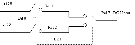
Relay 1 is closed for the motor to be driven in the forward direction.
For this to happen relay 7 has to be inactive so that the +12v can be connected
through the normal closed contact to the motor. To drive the motor in reverse
relay 1 should be open and relays 2 and 7 closed allowing the –12V through the
normally open contacts of relay 7.
Relays 2 and 7 are controlled by the same bit giving a complete path for
the –12V when the motor is requested to be driven in reverse. If the request is
made whilst the motor is travelling in a forward direction the motor will
change direction. If it is then stopped in reverse whilst control bit 0 is
active the motor will then drive forward again. Each motion should therefore be
stopped prior to the next one starting. The motor will be stopped in the
direction it is travelling when the associated limit switch is hit and a low
level signal is applied to the input of the digital I/O card via the ADC card.
When this is read the software toggles the control bit high opening the relay
and thus stopping the motor.
1.6.1.2: Shutter
Control
The shutter on the CCD module requires 24V volts to open it then 5V to
hold it open and closes when this holding voltage is removed. Relay 5 is
initially closed presenting 5V to the normally closed contacts of relay 8,
which is connected to the shutter. This however is not enough to open the
shutter. 24V is applied to the normally open contacts and the relay is momentarily
opened presenting 24V to the shutter allowing it to open. Relay 8 is then
closed again leaving the 5V holding voltage at the shutter. A capacitor is also
connected to the shutter line to hold a charge whilst relay 8 closes preventing
the shutter from closing before the holding voltage is connected as illustrated
below in figure 3. The shutter is closed by opening relay 5. When the shutter
opens a switch at the shutter closes, sending a low level input to the Digital
I/O letting the software know that the shutter has opened. If this signal is
not received relay 5 will be opened and the user will be informed that the
shutter failed to open.
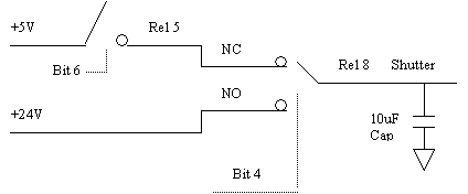
Figure 3 Shutter Control
1.6.2: Vexta Drive
card
The Vexta drive card is a bought in card to drive the Vexta 5-phase
motor on the beam splitter stage in the calibration unit. It requires 24V to
drive the motor and 5V for the logic circuitry. The card receives the 24V from
the power supply in the PSU module and the 5V from the VME crate along with the
drive signals from the VME-8 card. The drive card will then output 5-phase
signals to the motor in the required sequence to give the correct stepping.
1.6.3: Newport
Drive card 16-07e6.sch
The Newport drive card is an in house built card to drive the 2-phase
stepping motor attached to the Newport stage for the Deforrmable Mirror X
travel. This card also requires 24 and 5V supplies and produces 2-phase signals
in the correct sequence to drive the 2-phase stepping motor.
1.7: Berger Lahr Stepper
Motor Drive modules.
There are two Stepper drive modules each containing six drive cards made by Cortex Controllers used to drive all of the Berger Lahr 5-phase stepping motors. Drives 1-6 are in the top module and drives 7-12 are in the bottom module as they sit in the electronics rack. Table 2 above in the Motor controllers section (1.5.1) shows which drive controls which motor and hence which stage. The drive signals are supplied to the modules from the VME-8 and 44 cards and the modules then supply the motor phases with the correct stepping sequences.
1.8: FSM Filter : 16-07e1 to 3.sch
The Fast Steering Mirror (FSM) filter, filters the input signals to the FSM electronics from the Electra system. Its function is to protect the FSM from receiving demand voltages that are too high at the relevant frequency. The filter is made up of four LMF100 filters, each of which are dual 4-stage filters. A block diagram of the filter is illustrated below in figure 4.
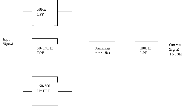
Figure 4 ; FSM Filter Block Diagram
Each of the individual filters use both parts of the LMF100 giving
8-stage filters. The cut-off frequencies are obtained by the resistor values in
the circuits. The output voltage of each filter is limited to different values.
There is no limitation on the 50Hz low pass filter, the 50-150Hz is limited to
4V and the 150-350Hz is limited to 1V. These three filters were used to
separate the frequency bands in order that they can be limited in this way. The
outputs of the filters are then summed together. The output of the summing
amplifier is effectively the output of the filter that corresponds to the
frequency being applied, hence if a signal of 30Hz is applied to the input it
will be allowed to pass through the 50Hz LPF but will be blocked by the other
two. The output of the summing amplifier will then be the same as the output of
the 50Hz LPF, which will be 30Hz, at whatever voltage was applied (limited to
+/- 6V due to the supplies). The output of the summing amplifier then goes to
another filter (300Hz LPF) which is the overall bandwidth of the FSM giving
additional protection from signals out with this range.
1.9: FSM Electronics
The FSM Electronics is the control unit for the fast steering mirror supplied from Zeiss with the mirror. The signals from Electra go through the above filter to this unit which then supplies high voltage signals to the mirror.
1.10: NCU Lamp PSU : 16-07e8.sch
The NCU lamp requires an igniter to start it, this is mounted in the calibration unit however the associated circuitry is in a box in the electronics rack. The power is switched on using a solid state relay which is controlled from output bit 2 of digital I/O card. When the relay is energised 240Vac is switched through a ballast and out to the igniter. The igniter then supplies a 4.5kV starting voltage to the lamp.
2: Calibration Unit : 00-07e5.dwg
The calibration unit consists of the following parts;
Mask stage
Beam Splitter Stage
Shutter
Lamp
Photodiode
Tip/Tilt Mirror
2.1 Mask Stage
The Mask stage is driven by the DC Motor controlled by the digital I/O
card via the relay card as previously described in section 1.6.1.1. Connections
go from motor and switches on the stage out to the connector panel on the side
of the calibration unit.
2.2: Beam Splitter stage
The Beam Splitter stage is a bought in unit driven by a Vexta 5-phase
stepping motor. It is controlled by the VME-8 card and driven by the Vexta
drive card in the PSU Module. There are
three switches on this stage, two limits (+/- direction) and a home switch,
which are all connected to the inputs of axis R of the VME-8 card.
2.3 Calibration shutter
The Shutter is driven by one of the Berger Lahr 5-phase motors to
control the intensity output from the NCU. The motor is controlled by the VME-8
card. There are no switches on this stage however a photodiode measures the
light from the lamp, which is controlled by the digital I/O card via the relay
card. The output from the photodiode is then connected via the BNC connector at
the side if the unit to the ADC card, where the analogue signal is converted to
digital and read by the Digital I/O card giving a reading of the light level.
From this the position of the shutter can be determined.
2.4 Tip/Tilt Mirror
The Tip/Tilt mirror is a small bought mirror with it’s own dedicated
controller situated in the electronics rack. It’s function is to allow testing
of the AO system by injecting a tip/tilt motion into the calibration image. Not
to be used in normal operation. The connections to the mirror are made from the
front of the controller to the connector panel of the calibration unit and
mirror. The unit was calibrated with these particular cables of the required
length.

3: Wave Front Sensor (WFS) : 00-07e2 to 4.dwg

![]()
The WFS, shown above in a simplified block diagram, contains a number
of stages that are driven by the Berger Lahr 5-phase stepping motors. Some of
the stages have encoders associated wirth them as detailed in table 2 (Motor
Controllers). All of the stages have Home or Limit switches associated with
them. All of the connections for the stages go to the connector panel at the
end of the WFS.
In the above diagram it can be seen that there are position, limit and
datum switches. The position switches are high precision switches used to Datum
the stages as well as act as a limit. The Datum switches are the same high
precision switches but are only used as a datum with the contacts connected to
the HOME input on the VME 8/44 cards. The limit switches are standard
micro-switches, the function of each of the switches are detailed below in
Table 5. The encoder heads are indicated by an “E”. There are three on the base
plate for each of the carriages and one for the Pick-off Y-stage. Each of the
encoder heads are connected to the associated encoder inputs on the VME 44
card, as shown in table 2.
|
Switch |
Purpose |
|
Position # 1 |
Acts as the datum for the Pick-off carriage and prevents the carriage
from hitting the end stop when travelling in the forward direction. |
|
Position # 2 |
Prevents the CCD Carriage hitting its end stop when in the Forward
direction. |
|
Position # 3 |
Acts as the datum for the Pick-off Y-stage and prevents the stage
hitting its end stop when travelling up (Forward) |
|
Limit # 4 |
Prevents the Y-stage hitting the lower limit (Reverse) |
Datum # 5 |
This switch is connected to the HOME inputs of the VME 8 card and
acts as a Datum for the filter wheel rotational stage. This has no affect
other than when there is a request to datum the stage. Hence there are no
limits. |
|
Datum # 6 |
The datum for the ADC # 1 rotation stage. |
|
Datum # 7 |
The Datum for the ADC # 2 rotation stage. |
|
Datum # 8 |
The Datum for the lenslet wheel rotation stage. |
|
Position # 15 |
Prevents the Fore-optics carriage hitting the pick-off carriage when
traveling in the reverse direction or similarly the if the pick-off is
travelling in the forward direction. If this switch is hit it will stop both
of these carriages. It also acts as the datum for the fore-optics carriage,
once the pick-off carriage has datumed the fore-optics carriage datum’s on
the pick-off carriage. |
|
Position # 16 |
Prevents the Fore-optics and CCD carriages from colliding. It will
stop both carriages, the Fore-optics when traveling forward and CCD when in
reverse. It also gives the datum for the CCD carriage. |
|
Limit # 20 |
Prevents the Pick-off carriage hitting its end stop when traveling in
the reverse direction. |
|
Limit # 21 |
Prevents the Fore-optics carriage from hitting its end stop when in
the forward direction. |
|
Limit # 22 |
Prevents the Fore-optics carriage hitting its hard stop when
traveling in the reverse direction. |
Table 5; WFS Switches
From the above table it can be seen that switch 15 will stop both the
Pick-off and Fore-optics carriage, however switch 1 will only stop the Pick-off
carriage in the same direction and switch 22 the Fore-optics carriage.
Similarly Switch 16 stops both the Fore-optics and CCD carriages but switch 21
will only stop the Fore-optics carriage. Additional logic circuitry, shown
below in Figure 6, has been added before the VME 8/44 cards to allow the
following functions;
Pick-off carriage
stopped in Forward direction by switch 1 OR 15
Fore-optics carriage
stopped in reverse direction by switch 15 OR 22
Fore optics carriage
stopped in Forward direction by switch 16 OR 21
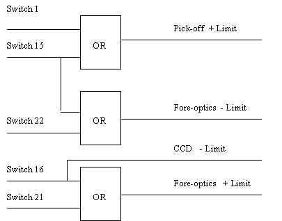
Figure 6; Switch Logic for WFS
With the above circuit each discrete fault condition due to switches
being hit will be the result of one single switch. For example;
The fore-optics stage can be stopped in the negative direction if switches
15 or 22 are hit and switch 1 or 15 will stop the Pick-off in the forwards
direction thus giving three possibilities that could stop these movements.
If the pick-off and fore-optics carriages both stop then switch 15 was
hit and the two carriages collided. If the pick-off stopped but not the
fore-optics then switch 1 was hit at the end of travel for the Pick-off,
similarly switch 22 will be hit if only the fore-optics carriage stops.
The CCD module consists of two CCD heads and two Peltier devices, which
are controlled by the CCD controllers. The connections for these are through
the side of the WFS. The connections for the shutter, which is also on the CCD
module is through the connector panel at the end of the WFS and is controlled
as previously described.
4: Optical Mechanical
Chassis (OMC) 00-07e6.dwg
The OMC sits on the optical bench and has the fast steering mirror,
which is connected to its dedicated controller in the electronics rack. The
deformable mirror also sits on a stage, which can be moved in the X and Y
directions. The stage is driven in the X direction by the Newport stage, which
includes two limit switches and an encoder. The Y direction is driven by one of
the Berger Lahr 5-phase motors controlled by the VME-8 card.
Appendix I
Spares List
2 x Berger Lahr Motors VRDM545
1 x Berger Lahr Motor VRDM566
1 x Position Switch
2 x Cortex motor drive cards. Drives 5 and 6 in the rack.
2 x NCU Lamps
1 x Igniter for NCU Lamp
1 x NCU Lamp holder
2 x Capacitors for NCU lamp PSU
To be Delivered;
1 x VME 44 Motor controller (With encoder inputs)
1 x VME 8 Motor controller
1 x MVME 167 Processor card
1 x MVME 712 Transition Card
1 x XVME 240 Digital I/O Card
Appendix II
Temporary setup of Eectronics rack
At present the rack is set up different from the layout described in
section 1, figure 1. The actual layout is illustrated below.
The EPICS record for the waveform generator card that would drive the
Tip/Tilt mirror has not been written therefore a signal generator is required
to apply a signal to the Tip/tilt unit so that the tip/tilt mirror in the
calibration unit can be driven. This however this mirror is not required for
normal operation.
The FSM has been sent back to Zeiss for repair so there is a substitute
FSM in the system at present controlled by the Tip/Tilt Amp at the top of the
electronics rack.