
Testing of SDSU Clock and Video Boards
There are two directories in the
/home/dspdev/ccd/timIII directory that contain code that can be
downloaded into an SDSU controller in order to test out the clock and
video boards. This code must not be used with a CCD attached, it would
almost certainly damage it. It is intended for use with a bare
controller only. The first directory 'VIDTST' contains code that
exercises the video board , the second ; 'CLKTST' exercises all the
clocks on the clock board. The code can be run using Voodoo , and each
directory conveniently contains a Voodoo set up file.
The CLKTST program
When this code is loaded into the controller it will immediately start driving all the clocks with a +/-10V amplitude square wave. The clock board must be configured with the correct address for this to work, this is done my ensuring that all the links JP1,3 and 4 are fitted and JP2 is off (these lie in a group of 8 close to the backplane ned of the board). The clock outputs should appear on pins 1 to 19 and 33 to 37, with pin 32 a ground). Running this program will require the utility card also to be fitted , since it does the power on.
The VIDTST program
The video cards each contain two independant channels . The video processor chains consist of a fixed gain front end followed by a switchable gain amplifier with 4 settings (x1,x2,x4.7,x9.5) followed by an integrator with a feedback capacitor of 2 selectable values (or 'speeds'). There are thus 8 combinations we must test to be thorough. This program runs through these combinations and returns an image divided into squares, each square corresponding to a combination. The program must be loaded, a special cable attached between clock card and video coax inputs and an image taken. It should appear thus:
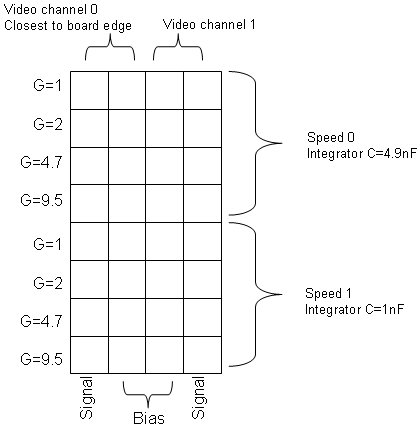
The left hand of the image is data from
video channel 0, the right from channel 1. The central part of the
image , from columns 50 to 100 shows how the bias level of the video
channel 0 varies as the various gain combinations are tried out.
Columns 101 to 150 show the same for the other video channel. The first
and last 50 columns show video amplifier response to the synthetic
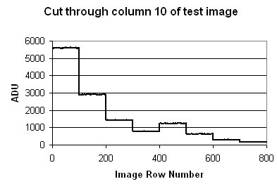
signal generated by pin 33 of the clock card. The graph below
shows what you should see in a vertical cut through either the first or
last 50 columns of the image. If you see this then the video amplifier
part of the board is probably OK. The peak should be in the region of
5000ADU. The upper part of the image should have the same staircase
appearance as the lower part but with an amplitude 5 times lower owing
to the larger integration capacitor in use.
The VIDTST program also checks out the DACs present on the video board
which are commonly used to bias the CCD output FET. These DACS are all
driven to their maximum values. Information on the voltages you can
expect on each pin are tabulated here.
The video card
should have links JP1,2,3,4 all set for this to work. Note that some of
the boards in the CCD39 WFS and INTWFC may have JP1 removed. If so ,
refit it temporarily.
For comparison, a fits image obtained
with the VIDTST program , using a working video board is shown here.
Simon Tulloch June 4 2008